


Mixer: main board
 1 -
1 - 
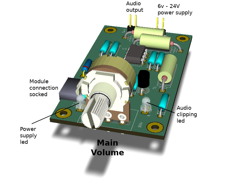 Figura 1: The main board for the modular audio mixer.
The main board contains the summing circuit, which takes care of mixing the audio signals coming from the different modules into a unique output. Moreover, it is the only one with power supply, and it provides voltage to all the other modules.
1 - Circuit characteristics
The elements on the user panel are:
- Power supply led: it shows that the device is on;
- Clipping led: it turns on when the mixer output exceeds the line voltage levels, that is, when the volume is too high;
- Main volume: it regulates the the mixer output volume;
The connections are:
- Audio output: the sum of all the audio inputs coming from all the input boards;
- Power supply: the single supply voltage; in the introduction to the mixer the allowed voltage range is discussed;
- Module connector: the connector to join the main board to all the other boards;
In the Figura 2 the variation of the main volume as a function of the potentiometer position is shown. The curve was plotted using the summing circuit formula in section 3.2, in case of two boards.
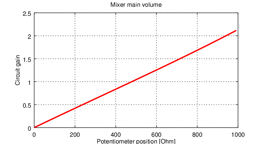 Figura 2: The variation of the main volume as a function of the potentiometer resistance, that is, as a function of its position. It can be noted that it is very linear.
2 - Assembly remarks
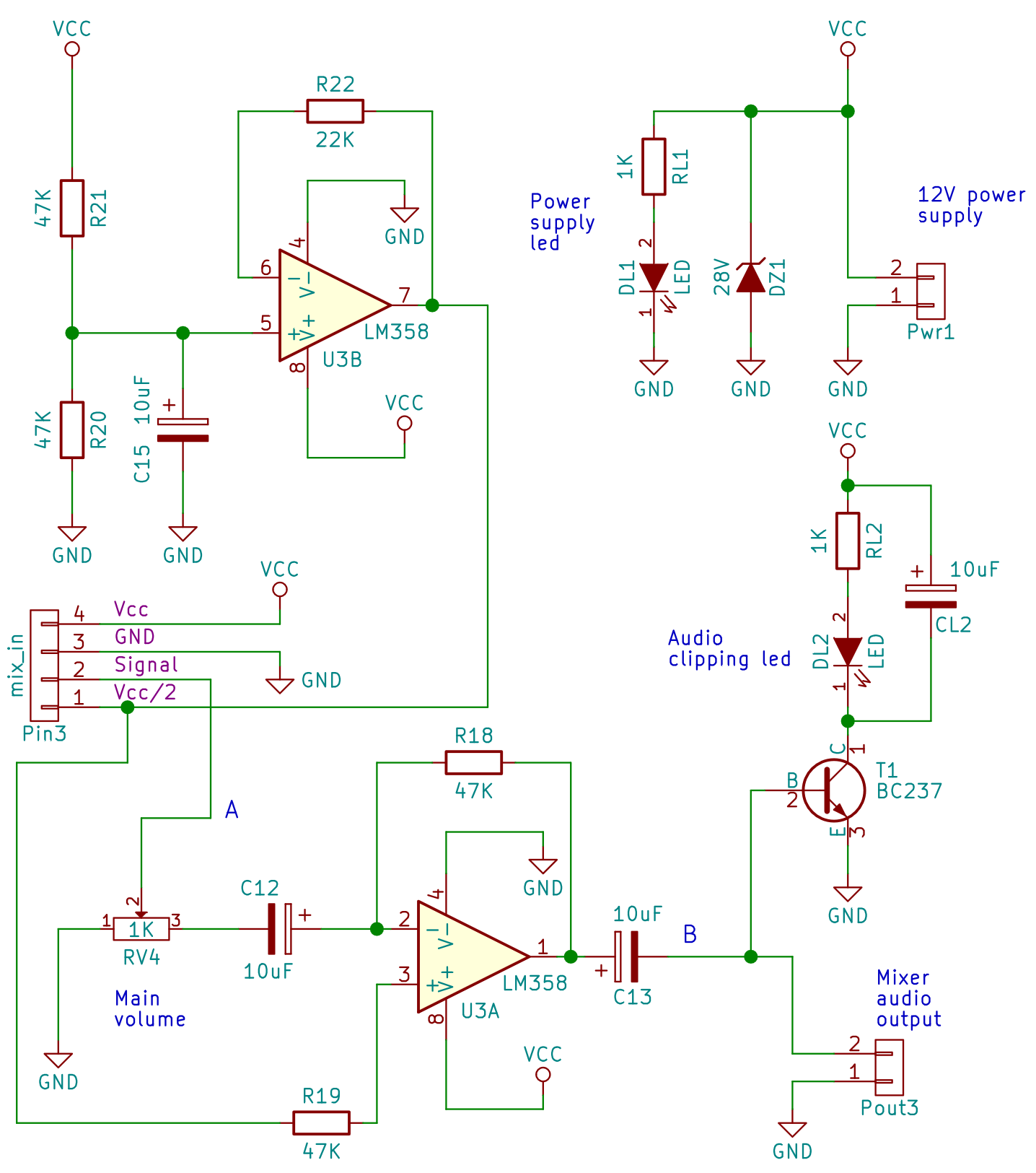 Figura 3: The schematic for the modular audio mixer main board.
The board assembly isn't difficult, and its dimensions are 4cm x 7cm, that are the standard size for a mixer module. To speed up the assembly or if not required, a few parts can be neglected and not soldered on the board. These parts are:
- DZ1 diode: without it the circuit won't be protected against overvoltage.
- DL2 clip led: this led shows the output audio signal clipping. If this feature is not required, CL2, RL2, DL2 and T1 can be omitted.
- DL1 power supply led: this led shows that the circuit is turned on. It can be omitted, together with its resistor RL1.
3 - The main board design
To understand the circuit functioning, the main board can be divided in different blocks with different purposes:
- The summing circuit;
- The volume potentiometer;
- The polarization voltage;
- The clipping led;
- The power supply led;
3.1 - The summing circuit
The heart of the mixer is a summing circuit, one of the most common configurations of an operational amplifier. Let's consider the standard setup, in case of single power supply, shown in Figura 4.
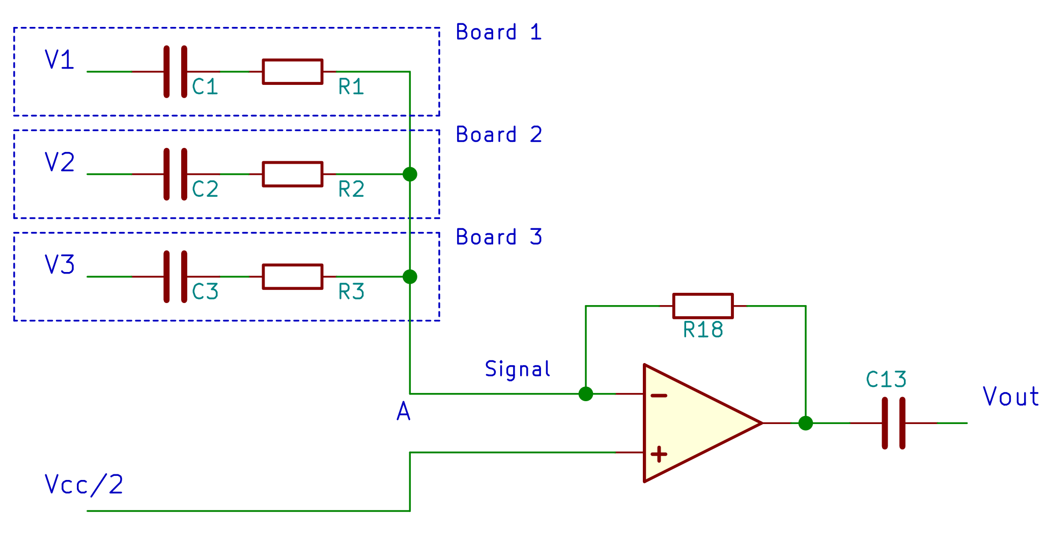 Figura 4: The theoretical schematic of a voltage summing circuit, made of an operational amplifier with a single power supply.
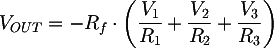
It can be noted that the branches for each input voltage all join together in the A node. The idea behind the modular mixer is to move all the components of each input branch (that is C1 e R1, C2 and R2, C3 and R3, etc) in the other boards, so that only one signal, called Signal in the schematics, has to go through all of them.
3.2 - The main volume potentiometer
In order to be able to regulate the main volume a potentiometer is required. Replacing the R18 feedback resistor with a potentiometer is not a good choice, for many reasons. It's better to insert the potentiometer between the opamp V- pin and the input branches coming from all the input boards, as shown in Figura 5.
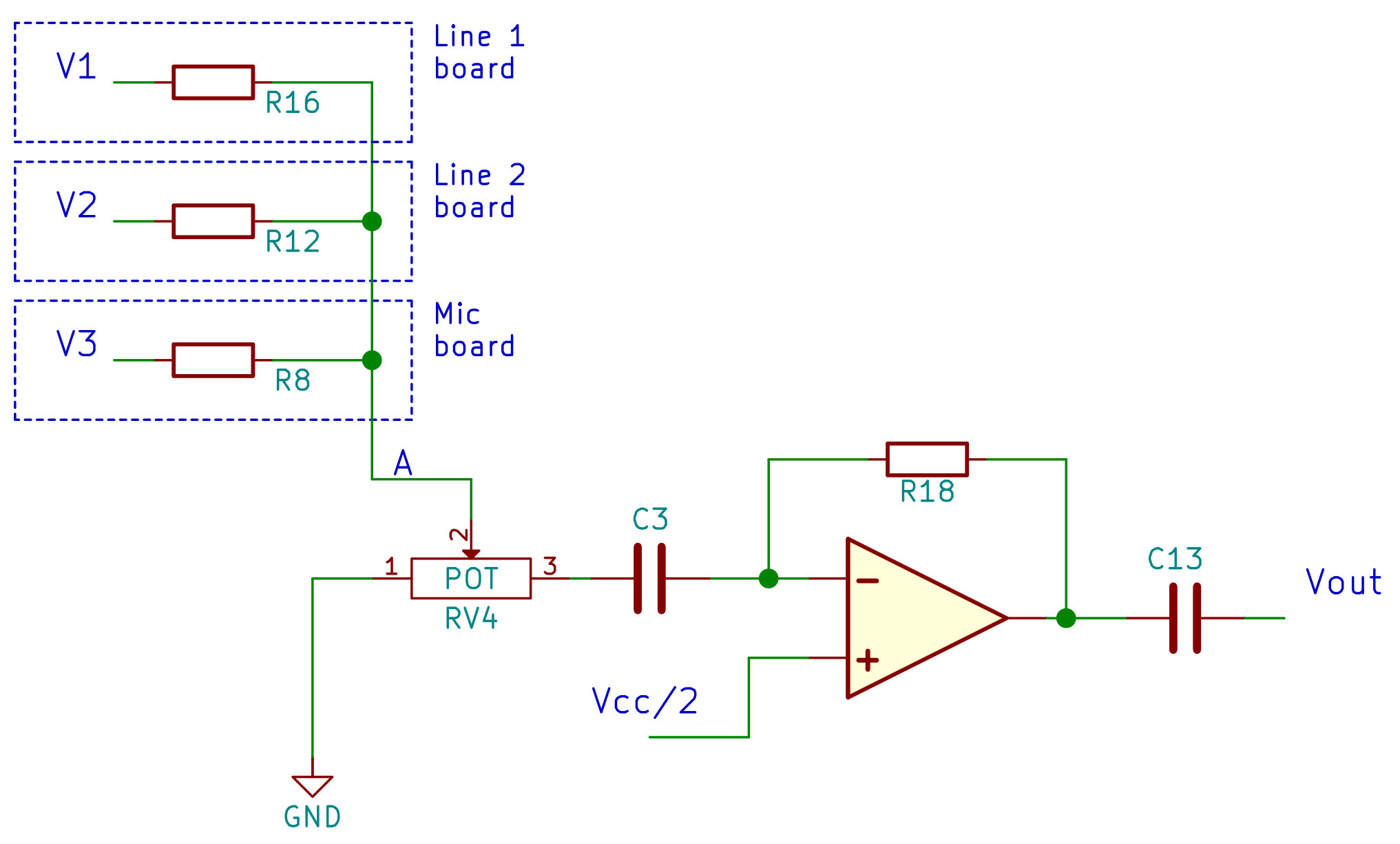 Figura 5: The schematic shows the modification to the previously shown summing amplifier schematic in order to include a volume potentiometer to control the mixer output volume. Differently from the former schematic, now the names of the components correspond to the final design ones.
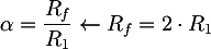
When the potentiometer shaft is turned towards pin 3, that is when the volume is at the maximum, the opamp output is connected directly to the input lines 1, 2, 3, etc, and therefore the circuit behaves exactly as the ideal summing circuit shown before in Figura 4. Moreover, the potentiometer resistance between pins 1 and 3 is connected to ground by the opamp V- pin, and therefore it has no effect. Let's put the summing circuit gain α equal to 2, in order to compensate the losses in the input modules or low input signals. Using the summing equations, we get:
 Choosing for example R18=47KΩ, we get R16=R12=R8=22KΩ
On the other side, when the potentiometer shaft is turned towards ground, there is no signal at the opamp input, and therefore the mixer output is zero. The exact formula for the output voltage when the potentiometer shaft is at an intermediate position is quite complex, and it is shown here only in case of two input lines, using Figura 4 as a reference:
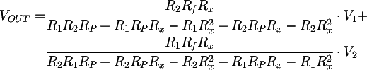 where RP is the maximum potentiometer resistance and Rx is a value between 0 and RP which represents the shaft position with respect to ground (that is, the resistance read between the potentiometer pins 1 and 2).
It can be noted that the gain for each input line, for example V1, depends on the resistances on all the other input lines, that is, it depends on R1 and R2. More generally, this means that adding input boards (that is, adding input lines 4, 5, etc,) the response of the potentiometers for each board changes. The more input boards are added, the less linear is the volume regulation, even if, as shown before, the minimum and maximum gains are constant. To reduce the non linearity due to adding input boards the main volume potentiometer resistance shoud be small, for example 1KΩ
where RP is the maximum potentiometer resistance and Rx is a value between 0 and RP which represents the shaft position with respect to ground (that is, the resistance read between the potentiometer pins 1 and 2).
It can be noted that the gain for each input line, for example V1, depends on the resistances on all the other input lines, that is, it depends on R1 and R2. More generally, this means that adding input boards (that is, adding input lines 4, 5, etc,) the response of the potentiometers for each board changes. The more input boards are added, the less linear is the volume regulation, even if, as shown before, the minimum and maximum gains are constant. To reduce the non linearity due to adding input boards the main volume potentiometer resistance shoud be small, for example 1KΩ
3.3 - Vcc/2 bias voltage
The UB3 is the heart of the circuit that creates the Vcc/2 bias voltage used for all the signals in the mixer. The circuit is a simple voltage follower, so:

The R21 and R20 resistors are a perfect voltage divider, since the opamp V+ pin isn't absorbing current. Choosing R21 = R20, the VIN voltage a the opamp V+ pin is half of the supplt voltage. Therefore VOUT is Vcc/2.
The R22 has to be equal to the equivalent resistance seen at the voltage follower input, that is at the V+ pin. In this way the negative effect due to bias currents at V+ and V- pins is minimized. The reasons for this choice are beyond the purposes of this article and are well documented on the internet, for example here: StackExchange: What is the purpose of a resistor in the feedback path of a unity gain buffer?. We therefore obtain:

The advantage of using an opamp to create the bias voltage, instead of a simple resistor divider, is that in this way Vcc/2 is supplied by an ideal source; the different input boards can absorb current from Vcc/2 without changing it. Said in other words, the Vcc/2 voltage at the resistor voltage divider is decoupled from the rest of the circuit.
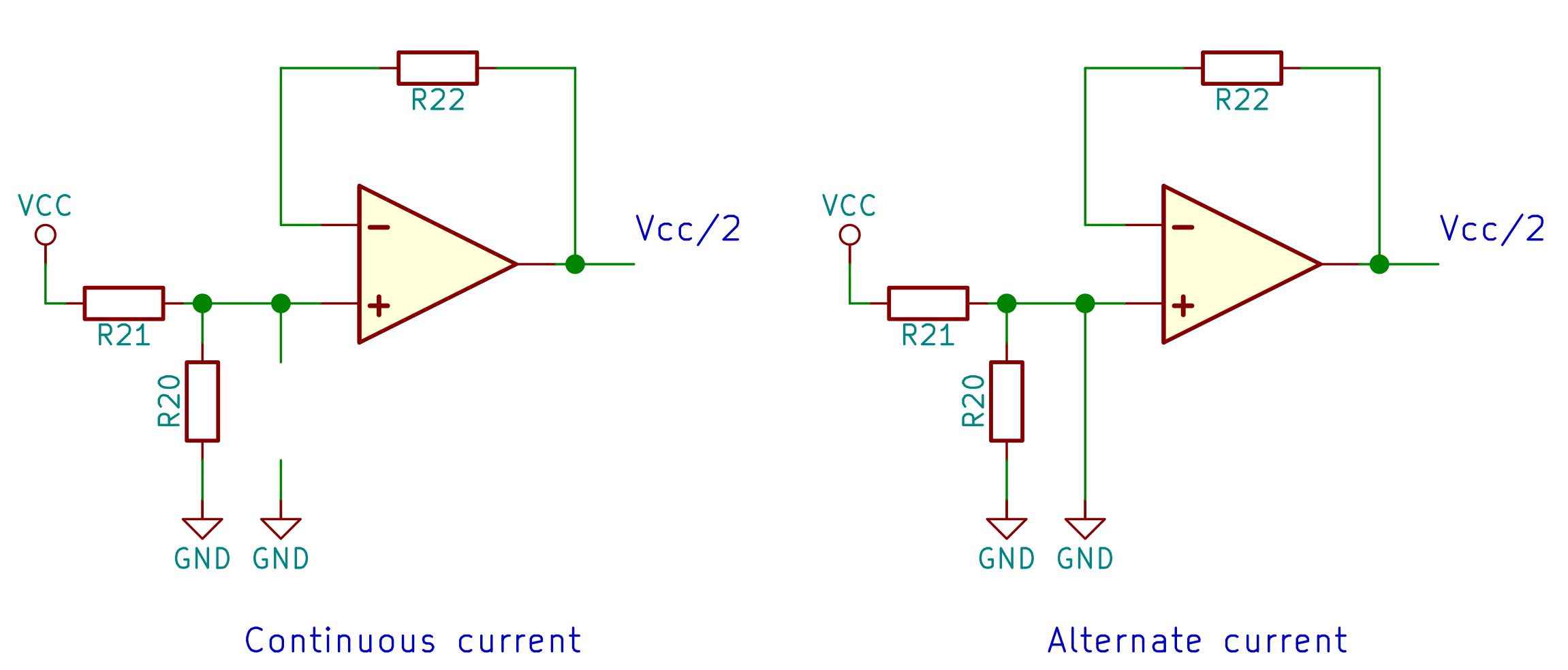 Figura 6: The behaviour of the C15 power supply ripple bypass capacitor, in case of continuous or alternate current.
The C15 capacitor reduces the noise in the circuit coming from the power supply, such as the residual ripple due to the AC voltage rectification. Indeed, from the point of view of an AC signal, the capacitor is a short circuit; the AC signals are therefore connected directly to ground and they don't enter into the the voltage follower. On the other side, from the point of view of the Vcc/2 continuous voltage the capacitor is an open circuit, and therefore it has no effect.
3.4 - The clipping led
The purpose of the DL2 led is to light on when the output signal is too high, that is, when there are distortions due to high volume. From an electrical point of view, the circuit, usually called "clipping circuit", has to turn on the output voltage is higher than 1V. To choose this voltage level we should consider that the mixer output is an audio line signal, which can be sent to any conumer audio device (a recorder, a mobile phone, etc). Even if there are international standards, the typical line audio levels are among 0.5V and 1.7V, as explained in the dedicated Wikipedia page. A reasonable value is therefore 1V.
T1 transistor has its base connected directly to the mixer audio output. The threshold voltage Vbe is, according to the datasheet, about 0.7V. This means that under 0.7V the transistor is not conducting. Since there is no resistor on the transistor base or collector, when the voltage exceeds the threshold the transistor saturates and it is, from the point of view of the led, a short circuit towards ground; a 10mA current (it will be calculated afterwards) will start to flow in the branch composed by the resistance, the led and the transistor.
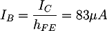
Assuming a minimum hfe=120, the base current is:
 that is a very low value. This means that connecting this simple circuit at the output of the U3A opamp doesn't affect the audio signal (the LM358 can supply about 30mA or 40mA maximum at its output).
The calculation of a resistor to be put in series to a led is well documented in literature and on the internet. We can write a Kirchhoff Voltage Law with the voltage VLED on the led, the voltage VCE sat on the transistor and the voltage VRL2 on the resistor:
 Which becomes:
 Obtaining:
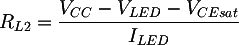 Considering BC327 datasheet, we can assume VCEsat=0.07V, Vcc=12V, ILED=10mA, VLED=2V, and therefore obtain RL2=1KΩ.
Finally, the capacitor CL2 is used to smooth the led response.
Considering BC327 datasheet, we can assume VCEsat=0.07V, Vcc=12V, ILED=10mA, VLED=2V, and therefore obtain RL2=1KΩ.
Finally, the capacitor CL2 is used to smooth the led response.
3.5 - The power supply circuit
The DL1 led is always on, since directly connected to the power supply, and it shows that the mixer is on. The led resistance calculation is similar to the one made in section 3.4 for the clipping led.
The DZ1 zener diode serves as a protection: since it is connected in reverse polarization, it is not conducting. If the supply voltage exceeds 28V, damaging the integrated circuits, the zener conducts and maintains the voltage at 28V, even if this means a high supply current and therefore a non recommendable situation.
Bibliography and other documents
Copyright 2014-2026 electroimc.com