


Subwoofer active low pass filter
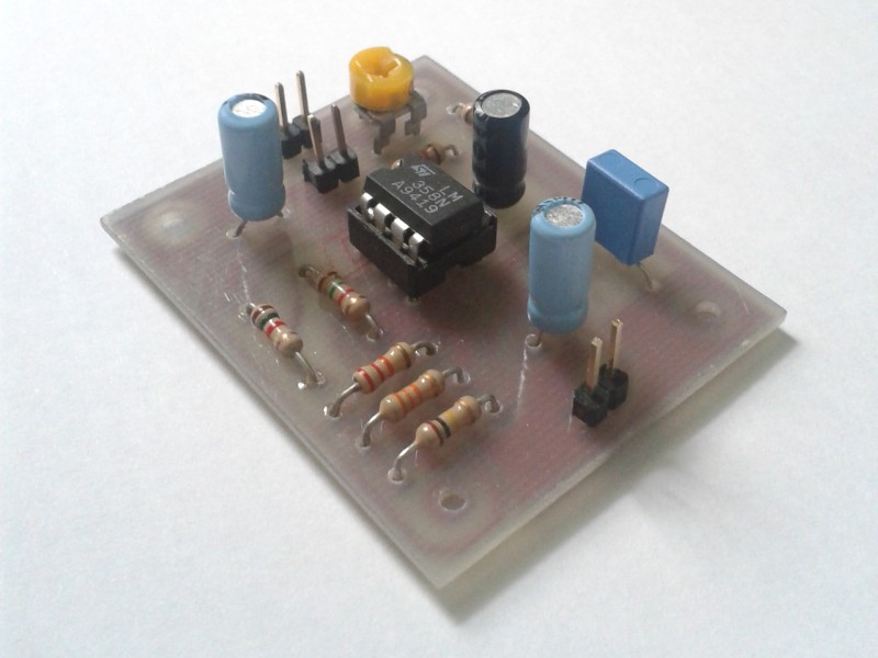 Figura 1: The subwoofer active low pass filter board.
This article presents a simple second order active low pass filter with an adjustable cutoff frequency between 20 Hz and 200 Hz. The circuit, which uses a single power supply, works on low power audio signal (that is, line audio levels) and is intended as a filtering element before a power audio amplifier driving a subwoofer loudspeaker. The design is based on the traditional Sallen-Key topology, which offers simple calculations and realization, though the quality factor isn't high. A simpler alternative to this circuit is the Subwoofer passive low pass filter.
1 - Circuit characteristics
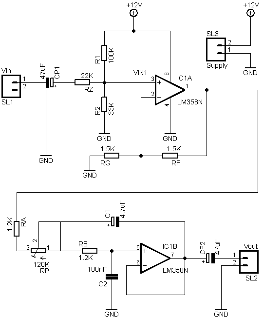 Figura 2: The circuit schematic
The filter behaviour was verified both through a LTSpice simulation and through a raw measurement with a PC soundcard and the Visual Analyser software. In the following images the modules of the transfer functions are represented in case of the potentiometer set on the lowest cutoff frequency (Figura 3), and maximum cutoff frequency (Figura 4). It can be notes that the two curves are basically equal, except at high frequencies, where the sound card low sensibility and noise don't allow for a precise measurement. The slope is always -40db per decade, due to the second order filter.
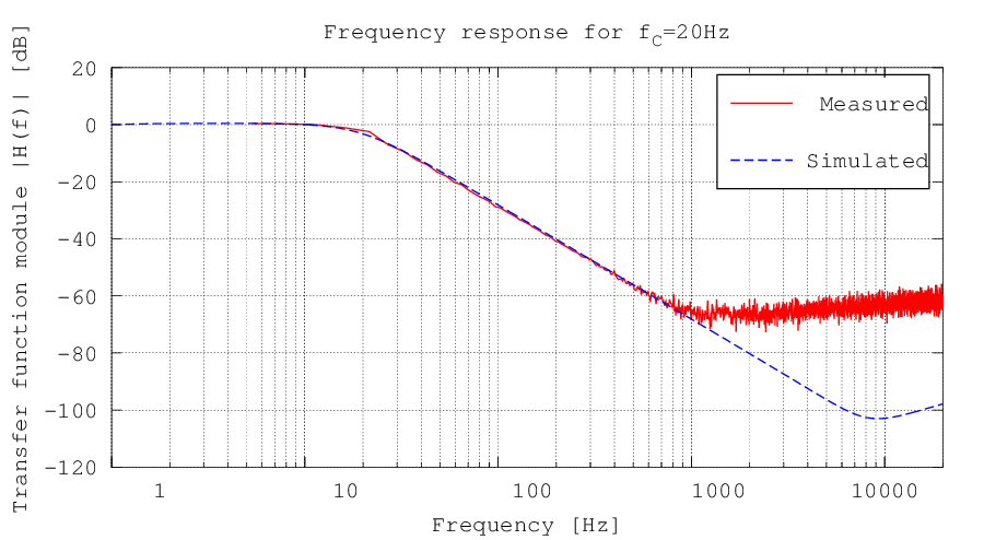 Figura 3: Circuit transfer function module in dB in case of a 20 Hz cutoff frequency, obtained through a measurement on the real circuit with a PC soundcard and the Visual Analyser software. The difference between the two curves at high frequencies is due to the low sensibility and noise of the computer sound card. On the abscissa a logarithmic scale was used.
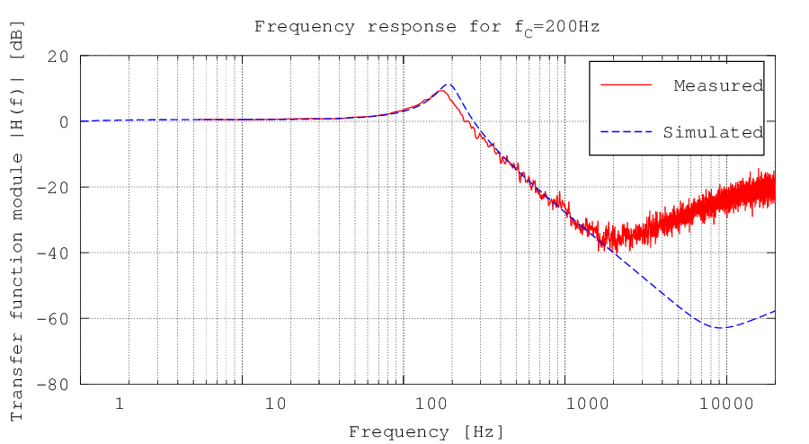 Figura 4: Circuit transfer function module in dB in case of a 200 Hz cutoff frequency, obtained through a measurement on the real circuit with a PC soundcard and the Visual Analyser software. The difference between the two curves at high frequencies is due to the low sensibility and noise of the computer sound card. On the abscissa a logarithmic scale was used.
A negative side of the filter is the badly balanced potentiometer: a linear variation of its resistance doesn't correspond to a linear variation of the cutoff frequency. Below the cutoff frequency as a function of the potentiometer resistance is plotted.
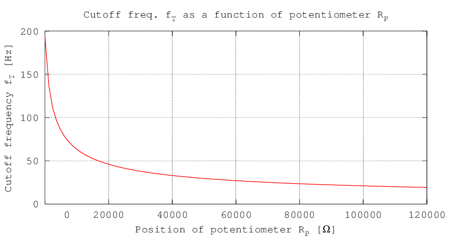 Figura 5: Frequency variation as a function of the potentiometer.
2 - Construction notes
The circuit realization is not difficult, since very common components were used, its size is small and its complexity is low. The board shown in figure 1 has a 4cm x 5cm sizes, and therefore it is a submultiple of the Eurocard european standard, which has a size of 160mm x 100mm. The connectors are three: one for the audio input, one for the audio output and one for the power supply.
 Download the complete KiCad project (68.3Kb)
Download the schematic, the printed circuit board, the Gerber files and the pdf for this proyect.
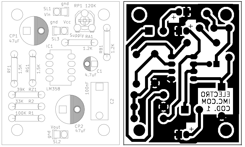 Figura 6: Silkscreen and printed circuit board for the filter.
3 - Stereo input modification
The circuit was initially designed to have a mono input. The lowest frequencies, inded, are usually the same on the right and the left stereo channels, sinsce our ears can't distinguish their spatial origin. For the same reason it's common to have two loudspeakers, one for the right side and one for the left side, for the middle and high frequencies, but only one subwoofer in a central position. Due to the requests in the comments, two solutions are proposed:
- Connect to the filter input only the left channel (L channel), since the bass signals are the same on the both channels;
- Modify the circuit as proposed in Figura 7;
For the circuit modification, the input resistance Rz and capacitor CP1 should not be soldered, and instead of them two resistors with the double of the value should be put, together with their decoupling capacitors.
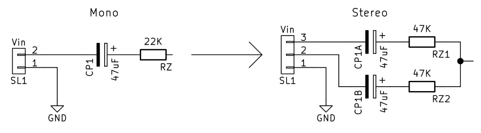 Figura 7: The modification for the filter input to obtain a stereo input. Rz and CP1 must be substituted with two resistors in parallel with the double of the value, together with their decoupling capacitors.
4 - The design: decoupling and polarization stage
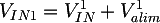
The first stage of the circuit is a non-inverting amplifier, which takes care of decoupling the filter input voltages and of biasing the signal by summing half of the supply voltage. In the traditional non-inverting amplifier VIN is connected directly to the op-amp non-inverting pin; in this configuration the gain is:
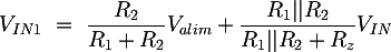
 In this case VIN is the voltage after the resistive network composed by R1, R2 and Rz. In order to calculate VIN1 we can use the effects superimposition, following a procedure similar to the one commonly used to solve the polarization in traditional BJT transistors circuits. The voltage will be the sum of two elements: the V1IN component, related to the input voltage VIN, and the V1alim, obtained from the Valim power supply voltage:
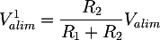
To find the V1alim value, we can consider the capacitor CP1 as an open circuit, since Valim is a direct voltage:
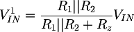
 While to determine the V1IN voltage we can consider Valim = 0V, and therefore we can substitute to the power supply a short circuit (as the superimposition method requires):
 Summing the two results we obtain:
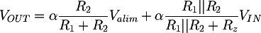
The gain of the non inverting amplifier is independent from the resistances which appear in the VIN1 expression, and therefore for simplicity we can put it equal to a constant:
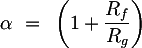 The total gain of the non-inverting stage is therefore:
4.1 - Choice of the components values
To find the components values, we can make some brief considerations: we decide that the VIN voltage is reported, unchanged, at the output; in order to polarize correctly the signal we must sum half of the power supply voltage to VIN; finally, we chose α=2, since this allows us to use RF = RG. Now we can write an equations system based on the VIN e Valim gains:
![Latex: \begin{cases} \alpha\dfrac{R_1 || R_2 }{R_1 || R_2 + R_z} = 1 \\\\[1em] \alpha\dfrac{R_2}{R_1+R_2} = \dfrac{1}{2} \\\\[1em] \alpha=2 \end{cases}](https://www.electroimc.com/it/img/formula/65069df682e9b5e0ea4beb0d0ccfc64df723f8c9.100.png) And, by solving it, we obtain;
And, by solving it, we obtain;
 To complete the information about the system we can compute the input impedance of the whole circuit:
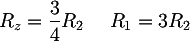
 Choosing R2 = 33 KΩ and keeping in mind the E12 series approximation, we obtain good values: R1 = 100 KΩ, Rz = 22 KΩ, Rin = 63 KΩ.
4.2 - The decoupling capacitors
The CP1 capacitor blocks the polarization current of the circuit, so that it doesn't flow into the device connected to the input. Said in other terms, it is a high pass filter with the following cutoff frequency:
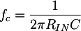 We impose that the cutoff frequency of this filter is much lower than the circuit minimum working frequency, for instance 1Hz. Since Rin = 66 KΩ, we obtain C = 2.5 uF. The 47 uF capacitor is therefore more than adequate the decoupling. Similar considerations can be done for CP2, substituting to Rin the load resistance; this resistance will be quite high, since it's the amplifier input.
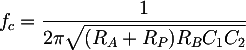
5 - The design: the filter
The following stage is the real filter. Many proofs exist on the web for calculating its transfer function, among which the Wikipedia one: Sallen-Key topology. Here it is:
 where RP is the value assumed by the P1 potentiometer. Analyzing this polynomial it's possible to extract some mathematical expressions useful during the design process.
5.1 - Design equations
If the denominator has two real poles, the Bode diagram of the transfer function will start to go down at the first pole with a -20dB/decade slope; at the second pole the slope will decrease down to the final value of -40dB/decade. If on the contrary the denominator has two complex conjugates poles, only one cutoff frequency will be present, with an asymptotic slope of -40dB/decade. This is the best condition for the filter. To obtain this from a mathematical point of view, we impose that the denominator has a negative discriminant:
 In this case, the cutoff frequency is:
To size the filter components, we can use the expression of its cutoff frequency. When the potentiometer is at the end or at the beginning, RP will be Rtot, which is the total potentiometer resistance, or it will be 0Ω. In these two cases the resulting cutoff frequencies will correspond to the minimum or the maximum allowed, that are f0 = 20 Hz and f1 = 200 Hz. The cutoff frequency formula reduce to:
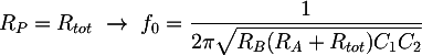
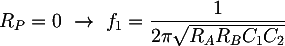 Substituting the limit frequencies and solving an equation system composed by the two previous equations we obtain:
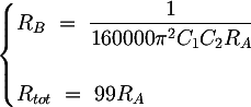
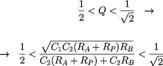
Another design condition can be obtained by the Q factor expression. If the transfer function has complex conjugate poles, resonance peak at the cutoff frequency might origin. To delete this peak, the filter quality factor Q must be limited:
5.2 - Graphical choice of the components values
Let's resume the useful equations written until now:
![Latex:
\begin{cases}
R_B ~=~ \dfrac{1}{160000 \pi^2 C_1 C_2 R_A} \\\\[1em]
%{R_{tot} ~=~ 99 R_A} \\\\[1em]
\left(\dfrac{C_2}{C_1}\right) < \dfrac{ 4 (R_A + R_P)R_B}{(R_A + R_P + R_B)^2} \\\\[1em] %Denominatore comune
\dfrac{1}{2} < \dfrac{\sqrt{C_1C_2(R_A+R_P)R_B}}{C_2(R_A+R_P)+C_2R_B} < \dfrac{1}{\sqrt{2}} \\\\[1em] %Fattore qualità
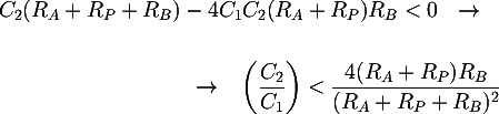
\end{cases}](https://www.electroimc.com/it/img/formula/dc4288aa846acb7a2579a2f74aef861812db5de2.100.png) In order, they are the equation obtained from the minumum and maximum cutoff frequency, the condition about the discriminant for having complex conjugate poles and the condition about the quality factor for avoiding resonance peaks.
In order, they are the equation obtained from the minumum and maximum cutoff frequency, the condition about the discriminant for having complex conjugate poles and the condition about the quality factor for avoiding resonance peaks.
The first of the three equations contains all the components values to be calculated. To choose them easily and intuitively the curve was graphically plotted, setting as parameters C1 e C2, RA on the abscissa and RB on the ordinate. On the same graph the area where the first inequality about the negative discriminant is true was coloured in green and yellow; the area coloured only in green is where the second inequality about the limited Q factor is verified. The two inequalities are evaluated assuming that the potentiometer has its maximum value, that is RP = Rtot = 99RA. The final graph, plotted with Derive 6, is shown in the following figure, in case of C1 = 4.7µF and C2 = 100nF:
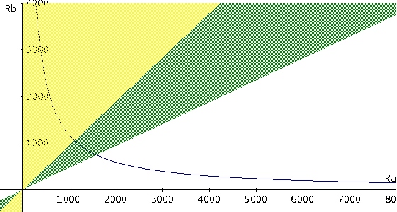 Figura 8: Graph used during the design phase to choose the filter components.
Bibliography and other documents
Copyright 2014-2026 electroimc.com